- ■
Samsung and ASML commit to 12-inch photomask transition, the first format change in decades
- ■
High NA EUV entering DRAM mass production by 2028—industry's first memory application at this scale
- ■
Transition removes stitching constraints and enables cost reduction through architectural change, not just process refinement
- ■
2028 timeline creates clear decision windows for chip buyers facing current memory shortage crisis
The semiconductor industry just crossed a manufacturing threshold it's been approaching for decades. Samsung and ASML announced today they're moving to 12-inch photomasks—the first format change since the industry standardized on 6-inch masks generations ago—while committing to High NA EUV lithography in DRAM production by 2028. This isn't incremental improvement. It's the industry acknowledging that continuing Moore's Law requires rebuilding fundamental manufacturing architecture, not just buying better equipment.
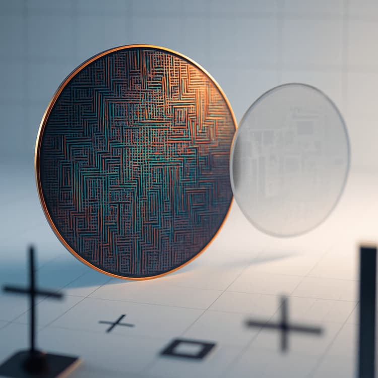
Samsung just committed to something the semiconductor industry has been circling for years: abandoning the 6-inch photomask format that's defined chip manufacturing for decades. The move to 12-inch masks, announced today alongside an expanded partnership with ASML, represents more than a specification upgrade. It's the clearest signal yet that continuing semiconductor scaling requires rebuilding the industry's manufacturing foundation from the ground up.
The numbers tell the story of why this matters now. Photomasks—the templates that define circuit patterns on silicon—have been stuck at 6 inches while wafer sizes grew to 12 inches. That mismatch created stitching constraints, where multiple mask exposures had to be precisely aligned to pattern a single chip. With High NA EUV lithography entering production, those constraints become deal-breakers. The physics of higher numerical aperture lenses means smaller field sizes, which would multiply stitching operations and kill productivity. Moving to 12-inch masks solves that problem while reducing manufacturing costs and increasing fab throughput.
But here's what makes this a genuine inflection point rather than routine equipment evolution: Samsung isn't just adopting new tools. The company announced it will bring High NA EUV into DRAM mass production by 2028—the first time this technology reaches high-volume memory manufacturing. That's the crossing point. Logic chips have been the EUV testbed for years. Memory manufacturers have watched, waited, and optimized around older lithography. This shift says the waiting is over.
The timing connects directly to the memory shortage crisis that's been building across AI infrastructure. Research teams are hitting compute walls not because of processor limits but because DRAM scaling stalled. Samsung's Vice Chairman Young Hyun Jun was explicit about the driver: "The AI era is transforming the semiconductor industry and increasing the importance of technological innovation across the entire value chain." Translation: AI workloads are breaking the old memory economics, and incremental improvements won't fix it.
High NA EUV brings improved resolution that enables process simplification—fewer lithography steps, higher yields, better economics at smaller nodes. For DRAM, that means extending the scaling roadmap that looked like it was hitting physical limits. The 2028 production timeline isn't arbitrary. It reflects the development cycles required for mask infrastructure, resist chemistry, and fab tooling to reach manufacturing readiness. Companies making memory procurement decisions today now have a concrete timeline for when relief arrives.
The strategic implications ripple outward from Samsung's move. TSMC has been the traditional EUV leader, deploying each new generation first in logic production. Samsung's commitment to High NA in memory manufacturing opens a different competitive dimension. Memory and foundry markets have different economics—DRAM lives and dies on cost per bit, while logic optimizes for performance and power. Proving High NA works in the cost-sensitive memory market validates the technology's manufacturing economics in ways logic production alone cannot.
For the broader industry, the 12-inch photomask transition creates a coordination challenge reminiscent of previous format shifts. Mask shops need new equipment. Inspection tools require updates. Supply chains must retool. ASML CEO Christophe Fouquet emphasized the partnership angle: "As the industry enters a new era driven by artificial intelligence, close collaboration with our customers becomes even more important." That's acknowledgment that no single company can drive this transition alone.
The capital requirements are substantial but unavoidable. High NA EUV systems cost upward of $350 million each—roughly double the price of current Low NA tools. Add mask infrastructure investment, and the barrier to entry rises significantly. That's creating a bifurcation point in the industry. Leading-edge manufacturers like Samsung, TSMC, and Intel can justify the investment to maintain Moore's Law scaling. Everyone else gets pushed toward trailing nodes or specialized processes where older equipment remains economically viable.
What's different about this transition is the explicit acknowledgment that it's necessary. Previous lithography generations—ArF immersion, first-generation EUV—were pitched as enabling better chips. High NA is being positioned as enabling continued chips. The framing shift matters. It reflects an industry that knows the easy improvements are behind it and the path forward requires fundamental architecture changes.
The 2028 timeline also creates clear windows for different market participants. Chip designers working on products launching in 2029 or later should be designing for High NA DRAM availability. Cloud infrastructure buyers can model their capacity planning around memory cost curves that start improving again after years of stagnation. Semiconductor equipment suppliers have three years to establish their position in the new photomask ecosystem.
For professionals in the industry, the transition redefines what expertise matters. Process integration knowledge around 6-inch masks becomes less valuable. Understanding High NA optics, new resist materials, and 12-inch mask handling becomes critical. The skill demand shift is already visible in job postings from leading fabs.
The announcement carefully avoids overpromising on timelines—Samsung says it "plans to introduce" High NA by 2028, not "will deploy." That's appropriate caution given the complexity involved. But the commitment itself matters more than the hedge. It tells the industry that the transition is happening, provides a target timeline, and creates pressure on the ecosystem to align around that schedule.
What we're watching is the semiconductor industry choosing to rebuild its manufacturing foundation rather than accept scaling limits. The 12-inch photomask shift and High NA DRAM production aren't separate developments—they're coordinated moves that together enable continued progress. The next two years will reveal whether the ecosystem can execute the transition on schedule or whether coordination challenges push timelines out.
The semiconductor industry just locked in its manufacturing roadmap through the end of the decade. For chip buyers, the 2028 timeline provides concrete planning horizons for when memory economics improve. For manufacturers outside the leading edge, this is the moment to decide whether to invest in next-generation capability or optimize around trailing nodes. Professionals should watch mask supplier announcements over the next six months—those will reveal whether the ecosystem can meet Samsung's timeline or whether coordination challenges emerge. The transition from 6-inch to 12-inch photomasks is the kind of industry-wide shift that happens once in a generation. It's happening now because continuing Moore's Law demands it.