- ■
Samsung and ASML expand partnership on High NA EUV, marking industry's first photomask format shift from 6-inch to 12-inch in decades
- ■
2028 target for High NA EUV in DRAM high-volume manufacturing—first concrete timeline addressing memory shortage crisis
- ■
12-inch photomask transition removes stitching constraints, increases fab productivity, signals infrastructure rebuild beyond incremental improvements
- ■
Memory-constrained AI buyers now have procurement planning window: relief arrives 2028
The semiconductor industry just crossed a threshold that's been decades in the making. Samsung and ASML announced today they're transitioning from 6-inch to 12-inch photomasks for High NA EUV lithography—the first photomask format change in decades. This isn't an equipment upgrade. It's proof that continuing Moore's Law requires rebuilding manufacturing infrastructure from the ground up. The concrete detail: Samsung will deploy High NA EUV in DRAM production by 2028, creating the first actionable timeline for enterprises managing memory shortages that constrain AI infrastructure.
Samsung just made the case that semiconductor advancement has shifted from evolution to revolution. The company's expanded partnership with ASML isn't just about buying next-generation equipment. It's about acknowledging that the industry needs to rebuild core infrastructure to keep Moore's Law breathing.
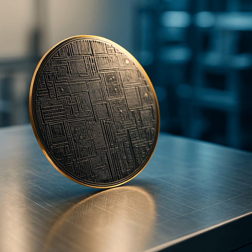
The photomask transition tells the real story. The semiconductor industry has used 6-inch photomasks for decades—literally the same format that's been printing circuits since the industry's formative years. Now Samsung is joining the initiative to move to 12-inch masks for High NA EUV lithography. That's not a process tweak. That's replacing fundamental tooling across the entire manufacturing chain.
Why does mask size matter? Because it determines how much of a chip you can pattern in a single exposure. The jump to 12-inch removes stitching constraints—the need to align multiple exposures to create larger patterns. According to Samsung's announcement, this increases fab productivity, lowers chipmaking costs, and enables manufacturers to fully leverage High NA EUV's capabilities. Translation: you can't just bolt new lithography machines onto old infrastructure and expect breakthrough results.
The 2028 DRAM timeline adds the second inflection point. Samsung plans to introduce ASML's High NA EUV into DRAM high-volume manufacturing by 2028—first in the industry. That's the earliest date memory-constrained AI infrastructure buyers can expect relief from current DRAM scaling limitations. Young Hyun Jun, Samsung's Vice Chairman and CEO, framed it clearly: "The AI era is transforming the semiconductor industry and increasing the importance of technological innovation across the entire value chain."
The memory angle deserves emphasis. AI training and inference workloads are hitting memory walls before they hit compute walls. High NA EUV extends the DRAM scaling roadmap through improved resolution that enables process simplification. Samsung's announcement notes this will support "increased efficiency"—corporate speak for "we can keep shrinking memory chips when current methods run out of room."
This mirrors the pattern TSMC established with logic chips, but memory manufacturing operates under different constraints. DRAM requires extreme uniformity across billions of identical cells. Any lithography improvement needs to work not just for cutting-edge processors but for memory arrays where a single defect can kill an entire chip. Samsung's dual role in memory and foundry manufacturing positions them to bridge both worlds.
The infrastructure rebuild extends beyond photomasks. High NA EUV requires new pellicles to protect masks, new resists to capture finer patterns, new metrology to measure smaller features. ASML's Christophe Fouquet noted that "close collaboration with our customers becomes even more important" as the industry enters this AI-driven era. That's acknowledgment that equipment vendors and chip manufacturers need to co-develop solutions rather than hand specifications over the wall.
For enterprise buyers, the 2028 date creates a decision window. Current DRAM technology can stretch through incremental improvements until then. But planning for AI infrastructure deployment in 2029 or beyond requires factoring in a step-function improvement in memory density and efficiency. That affects everything from data center design to cooling infrastructure to power delivery.
For chip manufacturers beyond Samsung, this announcement draws a line. Intel has High NA EUV machines on order. TSMC is evaluating deployment timelines. But Samsung just claimed first-mover advantage in DRAM, the segment where memory constraints hurt most. The 12-inch photomask initiative is industry-wide, but Samsung's commitment to 2028 production sets the pace everyone else needs to match or beat.
The cost curve matters too. Samsung's announcement explicitly calls out that 12-inch masks will "lower chipmaking costs." High NA EUV machines cost roughly $350 million each—double the price of current EUV systems. The only way that math works is if the entire manufacturing ecosystem becomes more efficient. Larger masks mean fewer exposures, fewer alignment steps, higher throughput. That's how you justify the capital investment.
What to watch: photomask infrastructure development timelines from suppliers like Hoya and Shin-Etsu. These companies need to build production capacity for 12-inch blanks before Samsung can deploy them at scale. Any delays there push the 2028 DRAM timeline right. Also monitor ASML's High NA system delivery schedule—they need to ship production-worthy tools 12-18 months before high-volume manufacturing begins.
The broader signal: this is what continuing semiconductor advancement looks like in 2026. Not iterative improvements but fundamental infrastructure transitions. The 6-inch photomask format served the industry through multiple technology nodes, multiple lithography generations, multiple chip architectures. Its replacement marks the moment when continuing down the roadmap required changing the roadmap itself.
For AI infrastructure buyers, 2028 just became the most important date on the memory roadmap. That's when Samsung's High NA EUV DRAM production provides the first architectural relief from current scaling limits. For chipmakers, the photomask transition signals that staying competitive requires infrastructure investment, not just equipment upgrades. Builders planning products for late-decade deployment need to factor in a step-function memory improvement. Investors should watch photomask supply chain development—any delays there cascade through the entire timeline. The next threshold: mask blank production capacity announcements from suppliers in the next 6-8 months will validate or challenge Samsung's 2028 target.