- ■
Samsung leads Mistral's Series D while deploying its models on-premises across semiconductor operations
- ■
AI shifts from design tool to production infrastructure—defect detection and equipment optimization now running in live fabs
- ■
On-premises requirement proves AI crossed security threshold for mission-critical manufacturing at nanometer scale
- ■
Creates recursive optimization: AI improves chip manufacturing, better chips enable more sophisticated AI, repeat
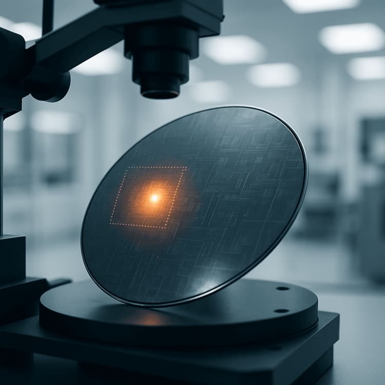
The recursive loop just closed. Samsung is deploying Mistral AI's large language models directly on semiconductor fab floors—not for marketing or customer service, but for defect detection, equipment optimization, and yield stabilization in the facilities building the next generation of AI chips. This marks the inflection where AI transitions from chip design consumer to manufacturing infrastructure, with hardware makers becoming both builders and deployers of AI in a self-reinforcing cycle that could reshape competitive dynamics across the $600 billion semiconductor industry.
Samsung just validated what semiconductor analysts have been watching for: AI sophisticated enough to optimize the manufacturing of AI chips themselves. The company announced it's integrating Mistral AI's flagship model, Mistral Large, across its fab operations while simultaneously leading the French company's Series D funding round. That dual move—investor and customer—signals something more significant than another enterprise AI pilot program.
The numbers tell the deployment story. Samsung's semiconductor division processes thousands of wafers daily across facilities in South Korea and Texas, each requiring precision measured in nanometers. According to Young Hyun Jun, Vice Chairman and CEO of Samsung's Device Solutions division, the company is applying AI models specifically to "defect detection and equipment optimization" to "accelerate development cycles, manufacturing precision, and yield stabilization across its advanced memory and logic chips." That's not exploratory language. That's production deployment.
What makes this transition technically significant: Samsung is running these models entirely on-premises. Not cloud-connected, not hybrid—fully contained within fab infrastructure boundaries. The company's official announcement emphasizes that on-premises solutions "ensure security and flexibility required to process highly sensitive technologies and operational data entirely within the boundaries of Samsung's semiconductor infrastructure, maintaining total control over its mission-critical technologies."
That security requirement proves AI capability crossed a critical threshold. Semiconductor fabs represent some of the most protected industrial facilities on Earth—billions in equipment, proprietary process recipes worth more than the hardware, and yields that can swing quarterly revenue by hundreds of millions. The fact that Samsung trusts AI models to run autonomously in this environment, processing operational data in real-time, marks a maturity milestone that extends far beyond semiconductors.
The recursive element creates the strategic inflection. Better AI models help optimize chip manufacturing. Those optimized processes produce better chips. Those better chips enable training more sophisticated AI models. And the cycle accelerates. Arthur Mensch, Mistral's co-founder and CEO, framed it directly: "AI is reshaping how we build complex technologies, from silicon to software... helping to improve how chips are designed and manufactured, and to accelerate technical progress across the global semiconductor and AI value chain."
This connects to broader industry patterns. TSMC has been deploying machine learning for yield optimization since 2019, but largely kept details proprietary. ASML, which builds the extreme ultraviolet lithography machines that enable cutting-edge chips, uses AI for predictive maintenance and process control. Samsung's public deployment with Mistral makes the transition explicit and sets enterprise expectations.
The timing aligns with manufacturing complexity hitting an inflection point of its own. As processes shrink toward 2-nanometer nodes and below, the number of variables in production multiplies exponentially. Traditional statistical process control can't handle the complexity at speed. Samsung's announcement acknowledges this directly: "As semiconductor processes become more advanced and complex, rapid data analysis in the fab is essential."
The Mistral selection carries geopolitical implications worth noting. Samsung could have deployed models from OpenAI, Google, or Microsoft. Instead, it chose a European AI company recently valued at $24 billion and backed this choice with Series D leadership. That decision reinforces AI sovereignty patterns we've tracked—major manufacturers preferring partners outside US Big Tech's immediate control, especially for infrastructure this critical.
For enterprise buyers evaluating AI deployment, Samsung's move provides a crucial data point. If AI can handle mission-critical operations in semiconductor fabs—where mistakes cost millions per hour and precision requirements exceed virtually any other industry—the security and reliability questions holding back deployment in less demanding environments lose weight. The on-premises architecture proves that sensitive operations don't require cloud connectivity or external model updates.
The competitive pressure just intensified. Samsung's public deployment means Intel and TSMC face questions about their own AI manufacturing optimization. Foundry customers selecting manufacturing partners will now ask about AI-enabled yield improvement and cycle time reduction. This becomes table stakes, not differentiation.
What we're watching next: time-to-market improvements and yield curve acceleration in Samsung's advanced nodes. If AI optimization delivers measurable advantages in 3-nanometer or 2-nanometer production ramps, every semiconductor manufacturer will face pressure to deploy similar systems within 12 to 18 months. The dataset advantage—years of fab operational data—means early movers could establish leads difficult to close.
Samsung's deployment transforms AI from chip design input to manufacturing infrastructure, creating a self-reinforcing optimization loop that could define competitive advantage in advanced semiconductors. For builders, the on-premises architecture validates that mission-critical AI doesn't require cloud connectivity. Investors should watch yield improvement metrics in Samsung's next earnings—evidence of AI manufacturing impact will accelerate enterprise adoption timelines. Enterprise decision-makers now have proof that AI can handle the most demanding operational environments, removing security objections for less critical deployments. The next threshold: public data on cycle time reduction and defect detection rates that quantify the advantage.